Solution for Parallel A/D Conversion Circuit of Image Sensor Chip Column
Overview
As the core front-end device of digital imaging systems, the performance of image sensors directly determines the imaging quality and system response speed. With the continuous improvement of demands for high-resolution and high-frame-rate imaging (such as 4K/8K video, high-speed machine vision, autonomous driving and other scenarios), the traditional single-channel A/D conversion architecture has been difficult to meet application requirements due to problems such as insufficient data throughput and superposition of transmission noise. The column-parallel A/D conversion circuit configures independent or shared A/D conversion units for each column of the pixel array to realize parallel quantization of analog signals, which effectively breaks through the speed bottleneck of the single-channel architecture, shortens the analog signal transmission path and reduces noise interference at the same time, making it one of the core solutions for high-performance CMOS image sensors. This paper will comprehensively elaborate on the solutions of column-parallel A/D conversion circuits for image sensor chips from the aspects of architecture selection, core technology design, typical implementation schemes, performance optimization strategies and application prospects.
Architecture Selection: Core Advantages and Classification of Column-Parallel Architecture
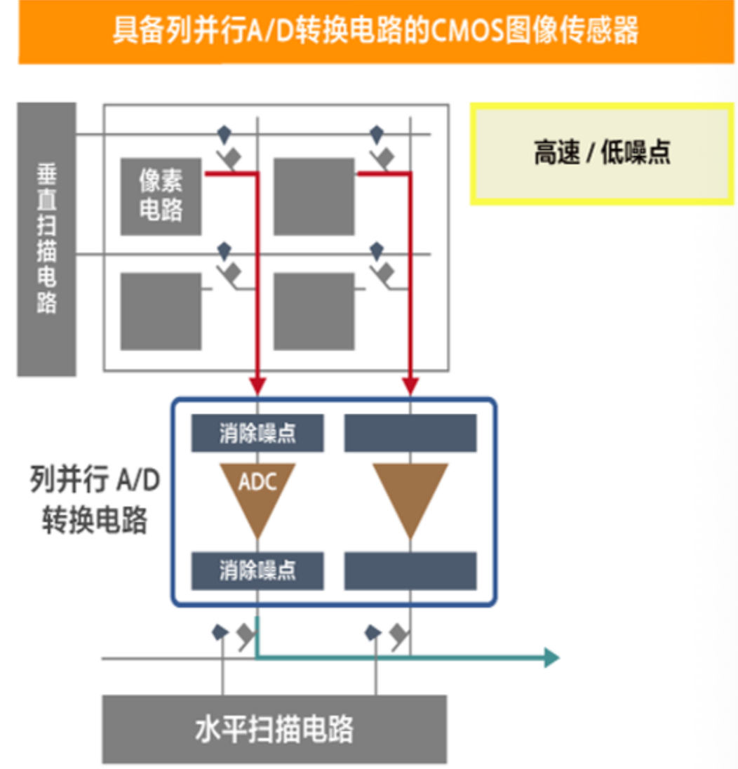
There are three mainstream schemes in the A/D conversion architecture of image sensors: single-channel, column-parallel and pixel-parallel. In the single-channel architecture, all pixels share one A/D converter. Although it has a high fill factor and good imaging quality, its conversion speed is limited and cannot adapt to high-frame-rate requirements. The pixel-parallel architecture equips each pixel with an independent A/D unit, which has the fastest conversion speed, but has inherent defects such as low fill factor, high power consumption and high area cost. The column-parallel architecture balances the requirements of speed, power consumption and area, and its core advantages are as follows: first, parallel processing improves the frame rate—the A/D unit shared by each column can synchronously process pixel signals in the column, greatly improving data throughput; second, shortening the transmission path reduces noise—analog signals are quantized within the column, avoiding noise superposition and signal attenuation caused by long-distance transmission; third, strong process compatibility—it can be deeply integrated with CMOS processes, facilitating the realization of system-on-chip (SoC) design.
According to the type of core conversion unit, the column-parallel A/D conversion architecture can be divided into the following three categories:
1. Column-Parallel Single-Slope ADC (SS-ADC) Architecture
It adopts an extremely simple structure of "ramp generator + comparator + counter". All columns share one ramp generator, and each column is configured with an independent comparator and counter. During operation, the ramp generator outputs a monotonically changing reference voltage, which is compared with the analog signal of the pixel in the column. When the two are equal, the counter value is latched to complete quantization. This architecture features simple structure, compact area and low power consumption, making it the current mainstream column-parallel scheme, which is widely used in consumer-grade and industrial-grade image sensors such as mobile phones and security systems.
2. Column-Parallel Cyclic ADC Architecture
It achieves high-precision quantization through multiple iterative approximation, and its core units include a comparator, a multiplying digital-to-analog converter (MDAC) and a shift register. Each column is equipped with a set of cyclic conversion units, and the resolution is improved by repeating the "comparison-amplification-feedback" process. On the premise of ensuring medium speed, this architecture can achieve high-precision conversion of more than 12 bits, which is suitable for scenarios with high requirements for imaging quality such as medical imaging and professional photography.
3. Column-Parallel 1-bit Comparator Iterative Architecture
Each column is configured with a simple 1-bit comparator, and bit quantization is completed in stages during the pixel signal integration process (for example, 2 bits are determined in each stage, and 8-bit quantization is completed in 4 stages). This scheme greatly simplifies the comparator design, reduces area and power consumption, and is suitable for low-power and highly integrated intelligent image sensors.
Core Technology Design: Key Modules and Performance Assurance
The performance core of the column-parallel A/D conversion circuit depends on three key indicators: resolution (dynamic range), conversion speed (frame rate) and power consumption. The design difficulty lies in how to realize low-noise, high-precision and low-power parallel quantization within the limited column pitch. The following are the design points of the core modules:
1. Low-Noise Comparator Design
The comparator is the core unit of column-parallel A/D conversion, and its noise level directly determines the conversion accuracy. In the column-parallel architecture, the comparator needs to achieve low-noise performance within a compact area, and the main design strategies are as follows: first, adopt a high-gain single-ended comparator, reduce thermal noise and flicker noise by optimizing transistor size and bias current, and achieve a low noise level of 2.4e⁻rms under the pixel size of 3.24μm; second, introduce dynamic bias technology, control the bias current through switched capacitors, provide high gain in the conversion stage to ensure accuracy, and reduce the bias current in the idle stage to save power consumption. For example, the low-power dynamic bias comparator controlled by switched capacitors can reduce the average column power consumption to 63.2μW; third, adopt dual noise cancellation technology to accurately cancel the reset noise of analog circuits and the coupling noise of digital circuits, further improving signal purity.
2. High-Precision Reference Signal Generation
The stability of the reference signal directly affects the quantization accuracy. Especially when multiple columns share a reference source in the column-parallel architecture, it is necessary to ensure the consistency and temperature stability of the signal. The design points include: first, adopt a bandgap reference voltage circuit to generate a reference voltage unaffected by temperature changes, which can provide four groups of high-precision reference voltages for multi-column ADC sharing; second, optimize the ramp generator design—for the SS-ADC architecture, adopt a capacitor charging and discharging circuit driven by a current source, compensate for capacitor drift and current deviation through calibration technology, and realize a ramp signal with excellent linearity; third, introduce a gain adaptive structure, adjust the quantization step size based on switched capacitors, compensate for the influence of photon shot noise, and improve the dynamic range. After calibration, a 13-bit dynamic range can be achieved.
3. Timing Synchronization and Data Readout Control
The column-parallel architecture needs to ensure that the A/D conversion units of all columns work synchronously, and realize efficient data readout at the same time to avoid data conflicts. The key designs include: first, adopt a global clock synchronization mechanism, generate high-precision timing signals through a clock generator, control the synchronous operation of the ramp generator, comparator and counter, and ensure the consistency of multi-column quantization; second, design a bidirectional double-edge counter with a low number of transitions to reduce the switching noise of digital circuits and improve counting efficiency; third, adopt a multiplexer (MUX) to realize serial output of parallel data. For example, divide 8 column ADCs into one group, summarize them through an 8-bit MUX and output them from a single pin, balancing the contradiction between parallel processing and the number of pins.
4. Stacking Process and Integrated Design
With the continuous reduction of pixel size (such as 1.12μm), the column pitch is becoming more and more compact, and traditional planar integration is difficult to meet the circuit area requirements. The stacking process has become a key technology for column-parallel ADC integration: first, adopt a two-chip stacking architecture, integrate the sensor pixels (using customized sensor processes) and column ADC logic circuits (using advanced CMOS logic processes) on the upper and lower chips respectively, and realize efficient transmission of column signals through through-silicon vias (TSV). This architecture can reduce the column ADC area to 2.24×365μm²; second, introduce a three-layer stacking architecture, add a DRAM cache layer between the sensor layer and the logic layer to realize temporary storage of high-frame-rate data, which can achieve ultra-slow motion recording of 960fps at full HD resolution; third, adopt chip-on-wafer (CoW) bonding technology—for large optical format sensors, stack multiple logic chips on the sensor chip, and realize high-density connection through micro-bumps to improve area efficiency.
Typical Implementation Schemes and Performance Indicators
Based on the above core technologies, the industry has proposed a variety of mature column-parallel A/D conversion solutions covering different application scenarios from consumer-grade to professional-grade. The following are two types of typical schemes:
1. Low-Power Column-Parallel Gain-Adaptive SS-ADC Scheme
This scheme is designed for high-resolution consumer-grade image sensors and is implemented using TSMC 180nm process. Its core features are improving dynamic range through gain-adaptive technology and optimizing circuit structure to reduce power consumption. The key designs include: first, adopt the SS-ADC architecture, configure each column with an independent comparator and counter, and share a ramp generator; second, introduce a switched-capacitor gain-adaptive structure, adjust the quantization step size according to the pixel signal intensity, and compensate for the noise impact in low-light environments; third, adopt a dynamic bias comparator and a low-transition counter to reduce static and dynamic power consumption. Measured performance indicators: average column power consumption of 63.2μW, dynamic range of 13 bits (after calibration), random noise of 1.2e⁻, FoM₁ value of 1.08e⁻·nJ/pixel, FoM₂ value of 0.29e⁻·pJ/step. The 5-megapixel CMOS image sensor realized based on this scheme adopts SEC 90nm BSI process, with a total system power consumption of 135.8mW, meeting the low-power requirements of mobile devices such as smartphones and tablet computers.
2. High-Precision Column-Parallel Cyclic ADC Scheme
This scheme is oriented to high-speed and high-precision industrial vision and medical imaging scenarios, and is implemented using TSMC 0.18μm CMOS RF mixed-signal process. Its core is to improve resolution through a cyclic iterative architecture. The key designs include: first, configure each column with a set of 12-bit cyclic ADC units, including a high-gain comparator and an MDAC module; second, integrate a column-parallel correlated double sampling (CDS) circuit to eliminate pixel reset noise; third, adopt global synchronous timing control to ensure the parallel conversion synchronization of the 64×64 pixel array. Measured performance indicators: ENOB greater than 11 bits, single-column ADC area of 11254μm², CDS circuit area of 2042μm², total chip power consumption less than 90mW, and the sequential scanning frame rate of the 64×64 pixel array reaching 520fps, which can meet the high-frame-rate requirements of HD TV 1080p specification.
Performance Optimization Strategies: Trade-off Between Noise, Power Consumption and Area
The design of column-parallel A/D conversion circuit is essentially a trade-off among noise, power consumption and area. According to the requirements of different application scenarios, the following optimization strategies can be adopted:
1. Noise Optimization Strategy
For low-light imaging scenarios, adopt digital correlated double sampling (D-CDS) technology to eliminate reset noise and fixed-pattern noise; introduce multi-ADC redundancy design, assign a single pixel signal to two ADCs for parallel conversion, and reduce random noise through data averaging; optimize the transistor size of the comparator input stage to improve gain and reduce flicker noise.
2. Power Consumption Optimization Strategy
Adopt dynamic power management technology to turn off the ADC units of idle columns during frame intervals; optimize timing design to reduce the number of transitions of digital circuits; adopt low-voltage processes (such as 65nm, 40nm) to reduce power supply voltage and power consumption on the premise of ensuring performance.
3. Area Optimization Strategy
Simplify the structure of the ADC core unit, such as replacing the high-precision comparator with a 1-bit comparator iterative architecture; adopt stacking process to integrate ADC logic circuits and sensor pixels in layers, making full use of vertical space; reuse circuit modules within the column, such as sharing reference sources and clock drive circuits among multiple columns.
Application Prospects and Future Trends
As the core technology of high-performance CMOS image sensors, column-parallel A/D conversion circuits have been widely used in smart phones, security monitoring, industrial vision, autonomous driving, medical imaging and other fields. With the upgrading of application requirements, the following development trends will emerge in the future:
1. Higher Resolution and Frame Rate
Through the optimization of advanced processes (such as 3nm, 2nm) and stacking architecture, realize a resolution of more than 16 bits and a frame rate of more than 1000fps to meet the needs of ultra-high-definition video and high-speed motion capture.
2. Low Power Consumption and High Integration
Combine near-threshold computing, asynchronous circuit design and other technologies to further reduce power consumption; integrate AI accelerators with column-parallel ADCs to realize the integration of "perception-quantization-computation" and improve the performance of intelligent image sensors.
3. Multi-Dimensional Sensing Fusion
On the basis of the column-parallel architecture, integrate A/D conversion units for multi-modal sensing such as infrared and depth to realize parallel acquisition and fusion processing of multi-dimensional image data.
4. Extreme Environment Adaptability
For extreme environments such as automotive and aerospace, optimize the temperature stability and radiation resistance of the circuit to improve the reliability and robustness of the column-parallel ADC.
The column-parallel A/D conversion circuit effectively balances the requirements of resolution, frame rate, power consumption and area of image sensors through the parallel quantization architecture, and is the core solution for high-performance CMOS image sensors. Its design core lies in realizing efficient and accurate quantization of multi-column signals through low-noise comparators, high-precision reference signals, synchronous timing control and stacked integration technology. Different application scenarios need to select the appropriate architecture according to performance requirements (for example, SS-ADC is suitable for low-power scenarios, and cyclic ADC is suitable for high-precision scenarios), and obtain the optimal design scheme through the trade-off optimization of noise, power consumption and area. In the future, with the progress of processes and architectural innovation, column-parallel A/D conversion circuits will develop towards higher performance, higher integration and multi-dimensional fusion, providing stronger technical support for various intelligent imaging applications.
Technical Advantages and Innovation Points
1. Efficient Conversion Strategy
The segmented successive approximation combined with dynamic section selection reduces the conversion cycle by more than 30% compared with the traditional SAR, improving the energy efficiency ratio.
2. High Precision Realization
Oversampling + digital correction technology achieves 14-bit equivalent precision, meeting the stringent requirements of medical imaging, industrial testing and other scenarios.
3. Area Miniaturization
Through operational amplifier sharing, RSD algorithm and compact DAC design, the area of a single ADC is reduced by 40%, which is suitable for ultra-thin camera modules.
4. Strong Anti-Interference Ability
The fully differential structure and multi-layer shielding design improve the PSRR to 70dB, adapting to electromagnetic interference environments such as automotive electronics.
5. Flexible Performance Adjustment
Support dynamic resolution switching (such as 10-bit high-speed mode under strong light and 14-bit low-noise mode under low light), balancing performance and power consumption.
6. Good Process Compatibility
The architecture is compatible with 10–16-bit resolution, and adapts to various advanced processes such as BSI and Stacked, with long-term technical vitality.
The algorithm combining segmented successive approximation and dynamic section selection reduces the conversion cycle by more than 30% compared with the traditional successive approximation register (SAR), significantly improving the energy efficiency ratio. Dynamic section selection automatically adjusts the conversion interval by real-time monitoring the amplitude of the input signal, thereby improving the conversion speed.
The application of oversampling technology and digital correction algorithm achieves 14-bit equivalent precision, meeting the application scenarios with extremely high precision requirements such as medical imaging and industrial testing. Oversampling technology improves the signal-to-noise ratio by increasing the sampling frequency, while digital correction technology effectively compensates for the nonlinear error of the circuit. With the help of operational amplifier sharing, RSD algorithm and compact DAC design, the area of a single ADC is reduced by 40%, which is more suitable for ultra-thin camera modules. Operational amplifier sharing greatly reduces the chip area by reusing the operational amplifiers in the analog circuit. The fully differential signal processing structure and multi-layer shielding design improve the power supply rejection ratio (PSRR) to 70dB, making it have excellent anti-interference performance and able to work stably in strong electromagnetic environments such as automotive electronics.